
Electrical circuit solvers are typically a computationally light simulation technique when compared to other techniques such as finite element or finite difference methods. But the types of simulations run with circuit solvers tend to be very long transient simulations, with potentially tens or hundreds of millions of time steps to calculate specific characteristic values for a design. Signal integrity simulations require long transients to resolve the bitstream and assess the reliability of data transmission in the system. Ansys uses IBIS/IBIS-AMI based methods along with 3D field solvers to analyse cutting edge DDR/GDDR/PCIe-type designs, but not all signal integrity applications suit this style of analysis.
The Qi wireless charging standard [1] is predominantly focused on implementing power transfer with a resonant inductive approach but it also includes the ability to communicate between the devices. NXP/Freescale [2] and Texas Instruments [3] provide example implementations which modulate data onto the power transfer system by connecting/disconnecting small amounts of additional capacitance, resulting in a change in the frequency response and therefore a small change in amplitude in the charging system. The transmitting device can then filter and decode the information by measuring the waveform at the transmitter coil.
At a high level, the general design of the system is quite simple, making it reliable and cost effective to implement (modelled in Figure 1). The transmitter switches the primary transmitting coil, and the receiver rectifies the received power to be used by the device.
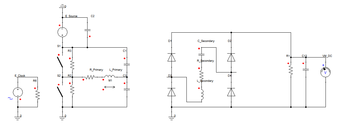
Figure 1 – High level Qi-based charger implemented in Ansys Twin Builder
The challenge with simulating this system is the wide disparity in frequencies. The power transfer signal is operating at 100kHz while the data transfer signal is operating at 2kHz. The power-focused part of the transmitter and receiver benefit from smaller time steps in order to resolve switching details in the semiconductors and therefore harmonic losses in the magnetic components. The data transfer system benefits from analysing long bit streams and a wide variety of operating conditions to determine the reliability of the transmitted data.
Implementing the required components to add modulation at the receiver and filter it at the transmitter considerably extends the basic design in scope, even without increasing the detail in the important components (extended circuit in Figure 2).
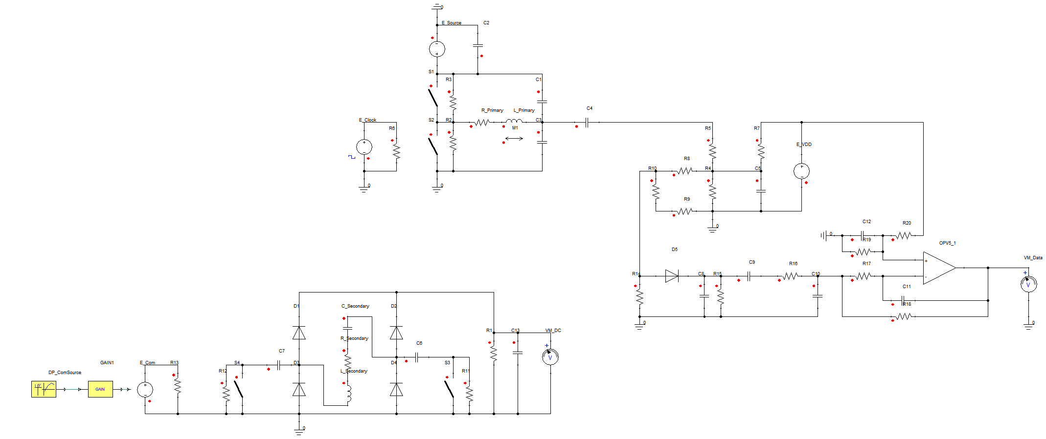
Figure 2 – Extended charger model with data system included
Running a complete analysis including both the power system and a suitable length of data (256 bits) requires 178ms, 50ms to reach a steady state in the system, and 128ms for the data sequence.
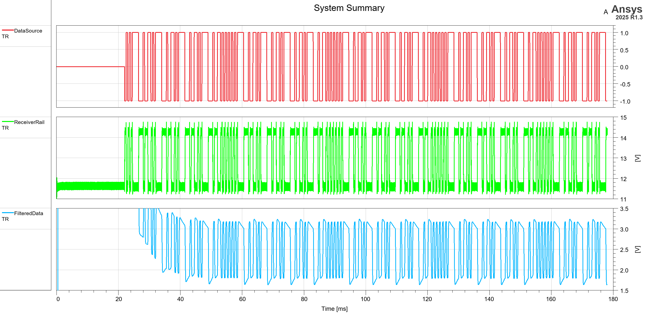
Figure 3 – Example transient data from a single simulation
There aren’t many opportunities for accelerating single solve simulations because of the transient nature of the solver, so the most common approach is to solve multiple variations in parallel wherever possible (i.e. multiple operating points or frequencies).
With the new Ansys optiSLang AI+ extension, there is an opportunity to train an AI model to replicate the data transfer part of the system and remove it from the circuit simulator entirely. A single simulation will then execute a short duration of the circuit simulator with the simpler model to determine the important power transfer characteristics (0.5ms instead of 178ms, using Figure 1 instead of Figure 2), while the trained AI model references the same circuit parameters to determine the important data transfer characteristics.
A wide variety of circuit parameters are exposed to the training process (resistance, inductance, capacitance, and coupling values). The full transient solution is captured (approximately 2.5 million time steps) and then resampled to standardise the time step size prior to being exposed to the AI model (reduced to 8900 time steps). The data capture process is automated in optiSLang, submitting batches of Twin Builder points to generate a total training set of 100 design points. The Deep Infinite Mixture Gaussian Process (DIM-GP) model is used to represent the voltage divider, rectifier, and low pass filter circuit and trained with the dataset.
As part of the training process, the model indicates which circuit parameters contribute to which parts of the waveform, filtering irrelevant parameters from the final result. Figure 4 shows a subset of the data supplied to the DIM-GP model. Figure 5 shows the total model accuracy in percent for the same domain (black line), and individual circuit parameters with the coloured lines (the coupling coefficient “k” being the dominant parameter). The correlation with parameters changes within a single bit and with different combinations of bits to represent the full waveform.
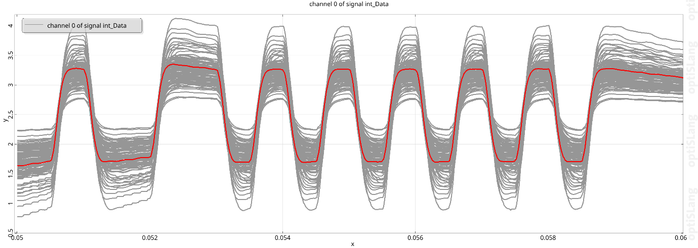
Figure 4 – Subset of input data for DIM-GP Model
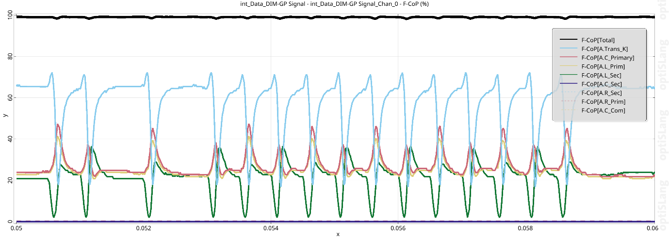
Figure 5 – Model parameter correlation with the input data
The most common way to interpret a long bitstream for system reliability is to postprocess the data into an eye diagram based on the data sample time. With some additional processing, the DIM-GP model can produce an eye diagram for each execution of the model and store it as an image in the optiSLang postprocessing file.
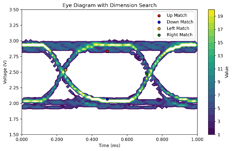
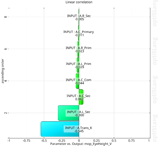
Figure 6 – Generated eye diagram with eye dimension measurement points labelled (left). Correlation coefficients between eye height and circuit parameters (right)
Just like with any other signal integrity analysis, the eye diagram can be measured to determine the key height and width metrics. This is added as a postprocessing stage after the DIM-GP model has been executed and it is integrated into the execution process (with the circuit parameter correlations for the eye height on the right).
This approach has significant improvements in speed for single simulations as well as larger design studies without requiring additional computing resources. All of the benchmarks were run on the same 8-core workstation with no other accelerators included. There was also no further optimisation of the execution process compared with the benchmark so any overheads to do with executing the project itself remain the same, making the improvements in Table 1 conservative. Much larger batches can now be executed with the potential for more acceleration.
The AI model is at least 150x faster than the original approach if only the data transfer performance is required. The hybrid configuration extracting power from the circuit solver and data from the AI model is at least 16x faster. If longer bit streams are required, the performance acceleration will only get larger because the DIM-GP model is designed for models with even larger datasets. The AI model is also transferrable to other circuit projects as long as the topology remains similar to the original training model.
Table 1 – Comparison of simulation time for 100 design points, with 5 simulations in parallel
| Solver | Time | Improvement |
|---|---|---|
| AEDT (Power + Data) | 1:13:48 | 1x |
| AEDT (Power) with AI+ (Data) | 0:04:41 | 16x |
| Only AI+ (Data) | 0:00:29 | 153x |
This is a new and emerging technology suitable for a wide range of simulation use cases. Feel free to reach out to our team at LEAP to discuss your specific project.
References:
[1] | Wireless Power Consortium, “Qi Wireless charging,” 20 June 2025. [Online]. Available: https://www.wirelesspowerconsortium.com/standards/qi-wireless-charging/. |
[2] | Freescale Semiconductor Inc., “Demodulating Communication Signals of Qi-Compliant Low-Power Wireless Charger Using MC56F8006 DSC,” March 2013. [Online]. Available: https://www.nxp.com/docs/en/application-note/AN4701.pdf. [Accessed 20 June 2025]. |
[3] | Texas Instruments Inc., “Qi Compliant Wireless Power Transmitter Manager,” September 2012. [Online]. Available: https://www.ti.com/lit/ds/symlink/bq500210.pdf. [Accessed 20 June 2025]. |